- This topic is empty.
-
AuthorPosts
-
2025-02-14 at 2:12 pm #8696
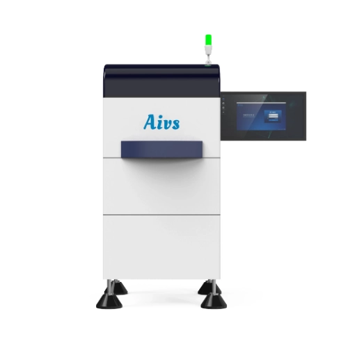
In modern electronics manufacturing, ensuring the quality and reliability of printed circuit boards (PCBs) is crucial. With increasing miniaturization and complexity of electronic components, manual inspection is no longer feasible. This is where Automated Optical Inspection (AOI) technology comes into play. AOI systems are designed to detect defects and ensure product quality efficiently. In this blog post, AlVS will share the working principle of 2D AOI auto optical inspection system, its components, advantages, and applications.
What is 2D AOI Auto Optical Inspection System?
2D AOI (Automated Optical Inspection) is a non-contact inspection method that utilizes high-resolution cameras and advanced image processing algorithms to inspect PCBs for defects. Unlike 3D AOI, which provides height information, 2D AOI relies on capturing detailed images of the board and comparing them against predefined standards to identify anomalies.
2D AOI is widely used in PCB manufacturing for detecting issues such as soldering defects, missing components, incorrect component placement, and other surface-level imperfections. The automated nature of the inspection process helps reduce human errors, increase production efficiency, and improve overall product quality.
Components of 2D AOI Auto Optical Inspection System
A 2D AOI system consists of several key components that work together to ensure accurate and efficient inspection:
1. High-Resolution Camera
The camera captures high-quality images of the PCB from various angles. The resolution of the camera plays a crucial role in detecting fine details and small defects.
2. Lighting System
Proper illumination is essential for highlighting defects. Different lighting techniques, such as LED lighting, multi-angle lighting, and structured lighting, are used to enhance image contrast and visibility.
3. Image Processing Software
The captured images are processed using advanced algorithms that compare the scanned PCB with a reference image or CAD data. The software identifies defects such as missing components, misalignment, soldering issues, and more.
4. Motion Control System
The PCB moves through the AOI system on a conveyor or fixed platform while the camera captures images. The motion control system ensures precision in positioning to achieve consistent inspection results.
5. User Interface and Data Analysis
The AOI system is controlled via a user-friendly interface that allows operators to configure inspection parameters, review detected defects, and generate reports for analysis.

Working Principle of 2D AOI Auto Optical Inspection System
The 2D AOI system follows a step-by-step process to inspect PCBs accurately. The working principle involves the following stages:
1. Image Acquisition
The inspection process begins with image acquisition, where the high-resolution camera captures images of the PCB under optimal lighting conditions. The camera can capture images from multiple angles to ensure a comprehensive view of the board.
2. Preprocessing and Image Enhancement
The captured images undergo preprocessing to enhance contrast, remove noise, and adjust brightness. This step ensures that the images are clear and ready for further analysis.
3. Pattern Recognition and Comparison
The system uses pattern recognition techniques to compare the scanned image with a reference model. The reference model is typically created from a golden board (a defect-free PCB) or CAD data. Any deviation from the reference is flagged as a potential defect.
4. Defect Detection and Classification
The AOI software identifies various defects, such as:
– Missing or misplaced components
– Incorrect component orientation
– Insufficient or excessive solder
– Solder bridges and short circuits
– Surface contamination or scratches
Each defect is classified based on predefined tolerance levels, and the severity of the issue is determined.
5. Decision Making and Reporting
Once the inspection is complete, the system generates a report highlighting the detected defects. Operators can review the results and take corrective actions, such as reworking defective boards or adjusting manufacturing processes to prevent recurring issues.
Advantages of 2D AOI Auto Optical Inspection System
1. High-Speed Inspection
2D AOI systems can inspect PCBs rapidly, significantly reducing the time required for quality control in high-volume production lines.
2. Enhanced Accuracy and Consistency
Unlike manual inspection, which is prone to human error, AOI systems provide consistent and reliable defect detection with high precision.
3. Cost-Effective Quality Control
By automating the inspection process, manufacturers can reduce labor costs and minimize the risk of defects reaching the final product, ultimately saving costs associated with rework and warranty claims.
4. Non-Destructive Testing
Since AOI is a non-contact inspection method, it does not cause any damage to the PCBs, ensuring that the tested units remain intact.
5. Real-Time Feedback and Process Optimization
AOI systems provide real-time feedback, allowing manufacturers to identify and address process variations early in the production cycle, improving overall manufacturing efficiency.
Applications of 2D AOI Auto Optical Inspection System
2D AOI technology is widely used across various industries that require precise and reliable PCB manufacturing. Some key applications include:
1. Electronics Manufacturing
Used in consumer electronics, automotive electronics, and industrial control systems to ensure high-quality PCBs.
2. Medical Devices
Essential for inspecting PCBs used in medical equipment where reliability is critical.
3. Aerospace and Defense
Ensures stringent quality standards are met in aerospace and defense electronics.
4. Automotive Industry
Helps maintain the reliability of electronic components used in modern vehicles, such as engine control units and infotainment systems.
Conclusion
The working principle of 2D AOI auto optical inspection revolves around advanced imaging technology and intelligent software to detect defects accurately and efficiently. By integrating 2D AOI systems into the manufacturing process, companies can enhance product quality, reduce defects, and optimize production efficiency. As technology advances, AOI systems continue to improve, offering even greater precision and automation capabilities for the electronics industry.
If you are in the electronics manufacturing industry, investing in a 2D AOI system can significantly enhance your quality control processes and ensure reliable products for your customers.
-
AuthorPosts
- You must be logged in to reply to this topic.